
Make your designs build-ready from day one.
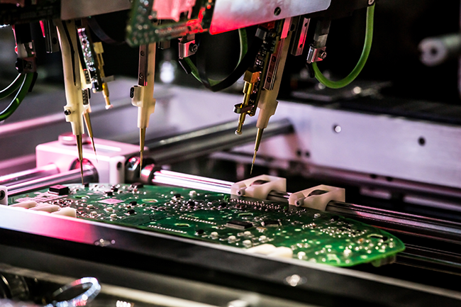
We bridge the gap between schematic, layout, and manufacturing. From DFM/DFT reviews to component strategy and PCB layout optimisation, our team helps your first build behave like revision three.

Design decisions aligned with real manufacturing and test constraints from day one.
Cost, lifecycle, and availability optimised for stable long-term production.
What We Do
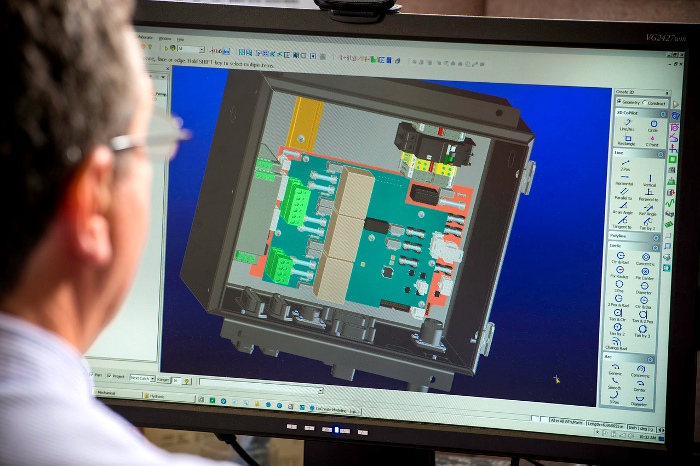
Our design engineering services bridge the gap between concept and production. We work alongside your team to optimise schematics, layouts and BOMs so your products flow smoothly into manufacturing.
With deep experience in circuit design, PCB layout and DFM/DFT analysis, we help you avoid costly redesigns, late-stage changes and unexpected line stops.
Our Design Optimization Process
A structured approach to convert early concepts into stable, production-ready designs.
Design Analysis
Comprehensive review of schematics, layouts and performance requirements.
DFM Optimization
Identify manufacturing risks and optimise for assembly and test.
Cost Reduction
Value engineering to reduce BOM and process costs.
Component Strategy
Component selection based on availability, lifecycle and performance.
Design Validation
Simulation, prototyping and validation for reliability and performance.
Release & Docs
Complete documentation package ready for manufacturing handoff.
Specialized Engineering Capabilities
Our team brings decades of experience across electronics design, manufacturing and optimisation. We leverage industry-standard tools and proven methodologies to deliver reliable, scalable outcomes.
Advanced PCB design & layout (Altium, Cadence, KiCad)
Signal integrity and power integrity analysis
Thermal management and long-term reliability analysis
EMC/EMI compliance & pre-compliance support
Firmware and software integration support
Supply chain and component lifecycle strategy
What We Offer
End-to-end design engineering services to make your products manufacturing-ready.

Circuit Design and Layout
Expert PCB design and layout services optimized for performance and manufacturability.

Design for Manufacturing (DFM)
Comprehensive DFM analysis to reduce costs and improve production efficiency.
Design for Test (DFT)
Testability analysis and optimization for easier quality control.

Component Selection
Strategic component selection balancing performance, cost, and availability.

Cost Optimization
Value engineering to reduce costs without compromising quality.

Technical Documentation
Complete technical documentation including schematics, BOMs, and assembly drawings.
Ready to make your design manufacturing-ready?
Share your schematics, PCB layouts and BOM. Our engineering team will respond with a structured DFM/DFT review, risk highlights and optimisation recommendations.