Introduction
Printed Circuit Boards (PCBs) are at the heart of every modern electronic product. From consumer gadgets to industrial automation systems, the reliability of the final product heavily depends on how well the PCB was tested during manufacturing. In India, where the EMS (Electronics Manufacturing Services) ecosystem is expanding rapidly, professional PCB testing has become a non-negotiable requirement.
In this article, we’ll look at the most widely used PCB testing methods by Indian EMS companies, when each method is used, and how to choose the right test strategy for your project.
Why PCB Testing Is So Critical
Even a minor defect on a PCB — a hairline short, weak solder joint, or missing component — can lead to field failures, costly RMAs, and damage to your brand image. Robust PCB testing helps you:
- Reduce DOA (Dead on Arrival) units
- Catch assembly and component defects early
- Improve long-term reliability and product safety
- Comply with industry and customer quality standards
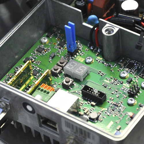
1. Visual Inspection (Manual and AOI)
Manual Visual Inspection
Manual inspection is still used for simple boards or low volumes. Operators check for visible defects such as:
- Missing or misaligned components
- Wrong polarity of diodes, electrolytic capacitors, LEDs
- Cold solder joints and bridges
- Contamination and physical damage
While cost-effective, manual inspection is operator-dependent and not ideal for dense SMT boards.
Automated Optical Inspection (AOI)
Most professional EMS companies in India now use AOI machines, especially for SMT lines. AOI uses high-resolution cameras and intelligent algorithms to detect:
- Solder bridges and insufficient solder
- Incorrect or missing components
- Misalignment and skew
- Wrong component orientation
AOI is fast, repeatable, and ideal for medium to high-volume production.
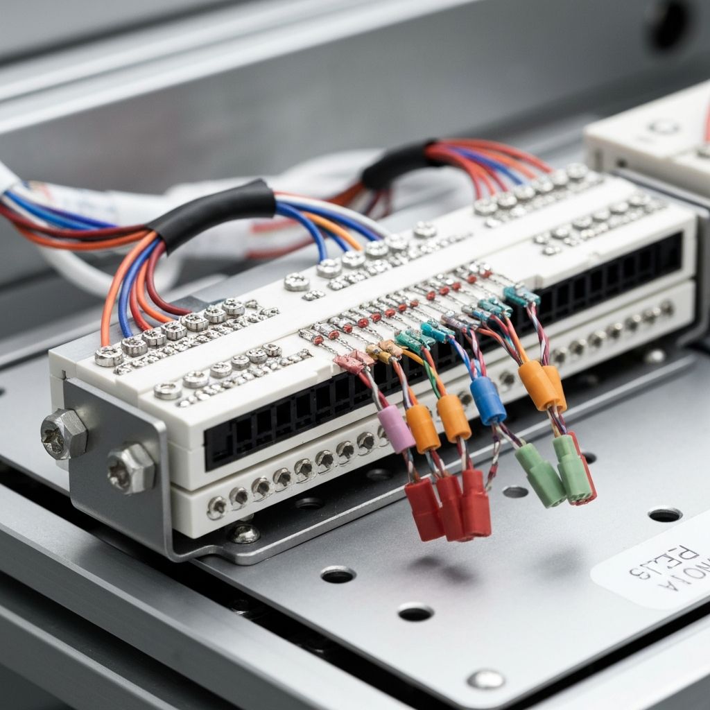
2. In-Circuit Testing (ICT)
In-Circuit Testing uses a “bed-of-nails” fixture or flying probes to make electrical contact with the PCB test pads and measure:
- Component values (resistors, capacitors, inductors)
- Presence and orientation of components
- Shorts and open circuits
- Basic functionality of some circuit blocks
ICT is highly effective for catching assembly defects early. However, it requires:
- Dedicated test fixtures (initial investment)
- Test points planned during PCB design (DFT – Design for Testability)
For stable, high-volume products, ICT quickly pays off due to its speed and fault coverage.
3. Flying Probe Testing
When volumes are lower or the design changes frequently, EMS providers often prefer flying probe testing instead of ICT. Here, moving probes touch different pads on the board under software control, without needing an expensive bed-of-nails fixture.
It is ideal for:
- Prototypes and pilot batches
- Complex boards with limited test pads
- Projects still undergoing frequent design revisions
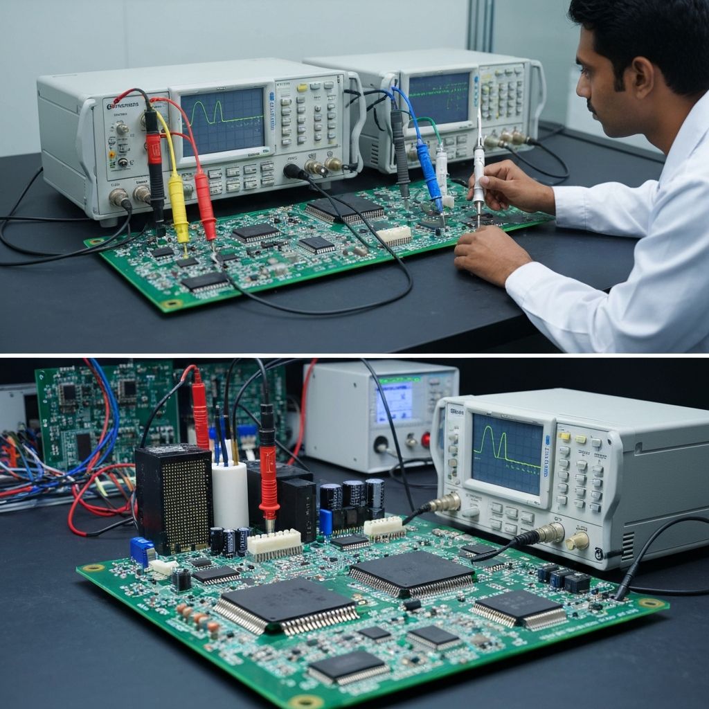
4. Functional Testing (FCT)
Functional Testing verifies whether the entire assembled PCB behaves like the final product. The board is powered up and tested using:
- Custom test jigs and fixtures
- Microcontroller programming and communication checks
- Sensor/actuator simulation and measurement
- Interface testing (USB, Ethernet, RS-485, CAN, etc.)
FCT is usually done after ICT or flying probe tests and ensures that the PCB works correctly in real-world conditions.
5. Boundary Scan (JTAG) Testing
For digital boards with FPGAs, microcontrollers, and high-pin-count ICs, JTAG boundary scan provides a powerful way to check connections between devices without physical test access.
Boundary scan is especially useful when:
- Boards are densely populated with fine-pitch BGAs
- Physical test pads are limited
- High-speed digital interfaces need structural verification
6. Environmental and Stress Testing
For critical applications (automotive, industrial, medical), EMS providers may also perform additional tests such as:
- Burn-in testing under elevated temperature and load
- Thermal cycling and humidity tests
- Vibration and mechanical shock tests
These tests ensure long-term reliability in harsh operating environments.
How to Choose the Right Testing Strategy
When working with an EMS partner in India, discuss:
- Your product’s target application and expected lifetime
- Volume (prototype, low volume, or mass production)
- Regulatory or customer-specific requirements
- Budget for fixtures and custom test setups
A good EMS provider will help you combine methods like AOI, ICT, and FCT to achieve high coverage at an optimal cost.
Conclusion
PCB testing is not just a formality — it is a strategic investment in your product’s reliability and brand reputation. By understanding the testing methods used by Indian EMS companies, you can better plan your design, budgets, and quality expectations from day one.